EVG ® 7300
EVG 7300
Multifunctional UV Nanoimprint Lithography System。Multifunctional UV Nanoimprint Lithography system up to 300mm featuring SmartNIL ® technology, lens molding and lens stacking in
广西科米瑞实验仪器设备有限公司提供 EV Group EVG 7300 产品资料、选型咨询、供货报价和售后服务支持,价格面议。
← 返回产品列表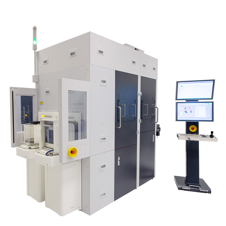
说明
Multifunctional UV Nanoimprint Lithography System
Multifunctional UV Nanoimprint Lithography system up to 300mm featuring SmartNIL ® technology, lens molding and lens stacking in one tool
The versatile EVG ® 7300 UV Nanoimprint Lithography System can support multiple related UV processes: SmartNIL, Wafer Level Optics (WLO) and Stacking – three capabilities merged in one flexible tool.
It is a standalone system based on the modularized and improved SmartNIL module, which can be configured depending on handling and automation levels. Supporting wafer sizes from 150 mm up to 300 mm and featuring high-precision alignment down to 300 nm, advanced process control and high throughput, the EVG ® 7300 can serve advanced R&D up to high-volume manufacturing (HVM) needs for a variety of freeform and high precision nano- and micro optical components and devices. For the necessity of integrated pre- and post-process flows in HVM environments, the module can be integrated into the HERCULES NIL system.
This multi-functional system is designed to serve a wide range of emerging applications involving micro- and nanoimprints as well as UV-stacking of functional layers. Thus, the equipment enables enhanced process performance for wafer-level optics (WLO), nanophotonics, metasurfaces and biomedical chips. This is closely related to the industry needs for novel optical sensors and optoelectronics to enable e.g. autonomous driving, micro lens arrays and projectors in automotive and decorative lighting, diffractive optics for biometric authentication as well as emerging trends for sophisticated meta-lenses. First applications utilizing this technology already exist today in the field of advanced biomedical devices and augmented reality waveguides where nanoimprinting enables high quality manufacturing of complex designs.
Features
Flexibility: UV-NIL system enabling three UV processes in one tool: SmartNIL, WLO and Stacking Precisely controlled multistep process including alignment, contacting and UV-curing Low-force automated stamp detachment for SmartNIL and WLO
Precisely controlled multistep process including alignment, contacting and UV-curing
Low-force automated stamp detachment for SmartNIL and WLO
Scalability: Processing wafers up to 300mm substrates
Modularity: Standalone module, as well integration into HERCULES NIL Substrate handling: from manual loading to fully automated operation Optional automatic stamp loading for SmartNIL allowing continuous mode operation
Substrate handling: from manual loading to fully automated operation
Optional automatic stamp loading for SmartNIL allowing continuous mode operation
Advanced Alignment Capabilities Live alignment <± 300nm (process dependent)
Live alignment <± 300nm (process dependent)
UV LED lamp up to high power 500mW/cm² > 90 % uniformity Optional: Dual wavelength operation: 365nm and 405nm Different exposure modes
> 90 % uniformity
Optional: Dual wavelength operation: 365nm and 405nm
提交需求
请填写必填信息,我们将在工作日尽快回复。