scia Cube 750
scia Cube 750
Products Ion Beam Etching Ion Beam Trimming Ion Beam Sputtering scia Cluster 200 more...
广西科米瑞实验仪器设备有限公司提供 scia Systems scia Cube 750 产品资料、选型咨询、供货报价和售后服务支持,价格面议。
← 返回产品列表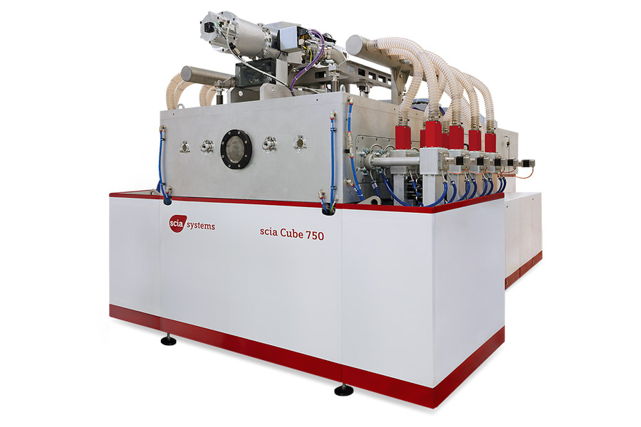
说明
Products Ion Beam Etching Ion Beam Trimming Ion Beam Sputtering scia Cluster 200 more...
Ion Beam Etching
Ion Beam Trimming
Ion Beam Sputtering
scia Cluster 200
Technologies
Applications Application Notes White Paper Publications Research Projects Learning
Application Notes
White Paper
Publications
Research Projects
Learning
Company About us News Events
About us
Contact Head Office Worldwide Visit us
Head Office
Worldwide
Visit us
scia-jobs.de
Large Area Coating and Etching over 750 mm x 750 mm
The scia Cube 750 is designed for large area high density plasma processes. The system enables deposition with high rates and a wide range of deposition parameters. In addition, etching processes with oxygen or halogen chemistry for high anisotropic etching and/or optimized selectivity are possible.
Features & Benefits
Large area processing with an array of synchronized linear microwave sources
Independent RF bias at substrate holder for energetic substrate bombardment
Substrate face-down orientation for minimized particle load
Substrate cooling (-10 °C)
In-situ chamber cleaning process
Full automation with vacuum load lock and atmosphere stocker system available
Need more Information? Contact us!
Applications
SEM picture of structured computer generated hologram (CGH) on a quartz sample with courtesy of IMS Stuttgart.
PECVD Processes Deposition of dielectric films, e.g. encapsulation, barrier coatings, electric insulation (SiO 2 , Si 3 N 4 , …) Optical and scratch resistant coatings (a-C:H, DLC)
Deposition of dielectric films, e.g. encapsulation, barrier coatings, electric insulation (SiO 2 , Si 3 N 4 , …)
Optical and scratch resistant coatings (a-C:H, DLC)
RIE Processes Reactive etching and structuring of metals (Ni, Cr, Pt, …) Etching of gratings and other structures in optical materials (quartz, fused silica) Ashing of photoresist
Reactive etching and structuring of metals (Ni, Cr, Pt, …)
Etching of gratings and other structures in optical materials (quartz, fused silica)
Ashing of photoresist
Application Note
Deposition of DLC for glass compression molds
规格
| 型号 | scia Cube 750 |
|---|---|
| Product category |
提交需求
请填写必填信息,我们将在工作日尽快回复。