scia Mill 300
scia Mill 300
Products Ion Beam Etching Ion Beam Trimming Ion Beam Sputtering scia Cluster 200 more...
广西科米瑞实验仪器设备有限公司提供 scia Systems scia Mill 300 产品资料、选型咨询、供货报价和售后服务支持,价格面议。
← 返回产品列表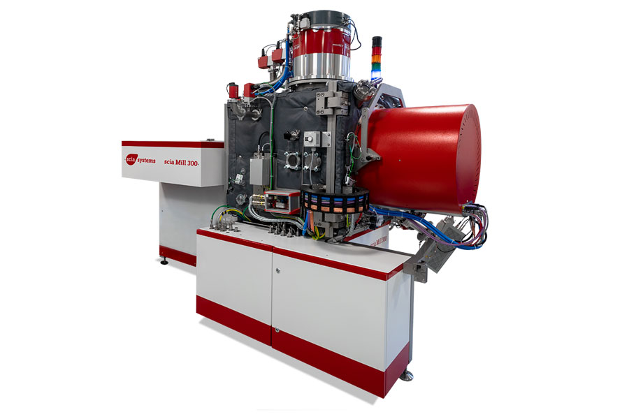
说明
Products Ion Beam Etching Ion Beam Trimming Ion Beam Sputtering scia Cluster 200 more...
Ion Beam Etching
Ion Beam Trimming
Ion Beam Sputtering
scia Cluster 200
Technologies
Applications Application Notes White Paper Publications Research Projects Learning
Application Notes
White Paper
Publications
Research Projects
Learning
Company About us News Events
About us
Contact Head Office Worldwide Visit us
Head Office
Worldwide
Visit us
scia-jobs.de
Structuring of Complex Multilayers on 300 mm Wafers
The scia Mill 300 is designed for ion beam etching of various substrate materials with up to 300 mm dia. Different end point detection systems allow accurate process control, and the system's full reactive gas compatibility enables reactive etch processes with improved selectivity and rate. Due to the flexible design of the scia Mill 300, the system can be used both for high-volume production with cassette loading as well as for small scale production with a single substrate load-lock.
Features & Benefits
Etching angle adjustment with tiltable and rotatable substrate holder
Excellent uniformity without shaper
Enhanced selectivity and rate with reactive gases
Process control with exact SIMS based or optical end point detection
Processing of wafers with photoresist masks due to good wafer cooling
Fully automatic cassette handling in variable cluster layouts including SECS/GEM communication
Need more Information? Contact us!
Applications
Reactive ion beam etching of slanted surface relief gratings (SRG) as optical couplers for Augmented Reality (AR). Left: Ion beam etching under different angles of incidence. Right: Etched quartz grating from principle and SEM result.
Structuring of magnetic memory (MRAM) and sensors (GMR, TMR, etc.)
Structuring of metals (Au, Ru, Ta, …), piezoelectric, and dielectric materials (PZT, KNN, AlScN, InP, Cu, Pt, Au, ...), e.g., for MEMS production
Delayering of multilayer structures for failure analysis
Patterning of waveguides (LiNbO 3 , BTO, …) for Photonic Integrated Circuits (PIC)
Production of slanted surface relief gratings (SRG) for Augmented Reality
Chemically Assisted Ion Beam Etching (CAIBE) of compound semiconductors (GaAs, GaN, InP, …)
Ion beam smoothing for reduction of microroughness
Surface Relief Gratings for AR- and MR-Devices
Magnetic Multilayers for tunnel-magneto-resistance (TMR) sensors
规格
相关产品
提交需求
请填写必填信息,我们将在工作日尽快回复。