scia Trim 300
scia Trim 300
Products Ion Beam Etching Ion Beam Trimming Ion Beam Sputtering scia Cluster 200 more...
广西科米瑞实验仪器设备有限公司提供 scia Systems scia Trim 300 产品资料、选型咨询、供货报价和售后服务支持,价格面议。
← 返回产品列表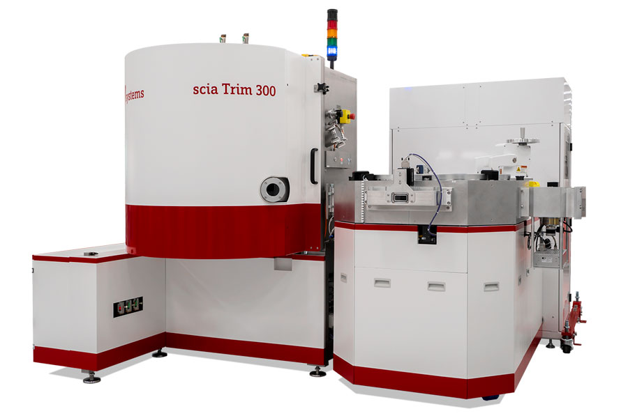
说明
Products Ion Beam Etching Ion Beam Trimming Ion Beam Sputtering scia Cluster 200 more...
Ion Beam Etching
Ion Beam Trimming
Ion Beam Sputtering
scia Cluster 200
Technologies
Applications Application Notes White Paper Publications Research Projects Learning
Application Notes
White Paper
Publications
Research Projects
Learning
Company About us News Events
About us
Contact Head Office Worldwide Visit us
Head Office
Worldwide
Visit us
scia-jobs.de
Precise Surface Correction by Ion Beam Trimming
The scia Trim 300 is a high-volume production system for ion beam trimming of 300 mm wafers without material restrictions. The precise local surface correction of the substrate is performed by a focused broad ion beam with a sufficient small focal point. Controlling the local material removal results in the etching of inhomogeneities up to an impressively uniform film, thus significantly increasing the yield of usable components.
Features & Benefits
Significant yield improvement
Film thickness uniformity to be adjusted down to atom level of 0.1 nm
No edge exclusion with electrostatic chuck
Sub-nanometer removal with zero base etch function
Processing of film and wafer materials without restrictions
Throughput and maintenance optimized design for low production costs
Processing of wafers with photoresist masks due to good wafer cooling
Need more Information? Contact us!
Applications
Results IBT
Results (left-pre, right-post) for ion beam trimming of SiO 2 on a 300 mm wafer. Standard deviation: pre: 1.3 nm, post: 0.3 nm; Improvement factor: 4.3; Average thickness: pre: 1010.7 nm, post: 955.1 nm; Removal: 55.6 nm
Frequency trimming of bulk acoustic wave (BAW) or surface acoustic wave (SAW) filters
Film thickness trimming of silicon on insulator (SOI) and piezo material (LT, LN) wafers
Dimensional correction of waveguides for photonic integrated circuits (PIC)
Structuring of slanted surface relief gratings (SRG) on master stamps for imprint technologies
Dimensional correction of MEMS structures
Form error correction for X-ray mirrors
Thickness Trimming for PIC (Photonic Integrated Circuit) Wafers
规格
| 型号 | scia Trim 300 |
|---|---|
| Product category |
相关产品
提交需求
请填写必填信息,我们将在工作日尽快回复。