ComBond ®
ComBond
Automated High-Vacuum Wafer Bonding System。High-vacuum wafer bonding platform facilitating covalent bonds of “anything on anything”
广西科米瑞实验仪器设备有限公司提供 EV Group ComBond 产品资料、选型咨询、供货报价和售后服务支持,价格面议。
← 返回产品列表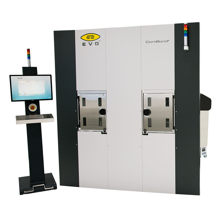
说明
Automated High-Vacuum Wafer Bonding System
High-vacuum wafer bonding platform facilitating covalent bonds of “anything on anything”
The EVG ComBond high-vacuum wafer bonding platform marks a new milestone in EVG’s unique portfolio of wafer bonding equipment and technology in response to market needs for more sophisticated integration processes. The application areas supported by the EVG ComBond range from advanced engineered substrates, stacked solar cells and power devices to high-end MEMS packaging, high-performance logic and “beyond CMOS” devices. The modular cluster design of the EVG ComBond system allows for a highly flexible platform that can be tailored to various demanding customer needs both in R&D and high-throughput, high-volume manufacturing environments. The EVG ComBond facilitates the bonding of heterogeneous materials with different lattice constants and coefficients of thermal expansion (CTE) as well as the formation of electrically conductive bond interfaces by its unique oxide-removal process. The EVG ComBond high-vacuum technology also enables low-temperature bonding of metals, such as aluminum, that re-oxidize quickly in ambient environments. Void-free and particle-free bond interfaces and excellent bond strength can be achieved for many material combinations.
Features
High-vacuum, aligned, covalent bonding Processing in high-vacuum environment (< 5·10 -8 mbar) In-situ sub-micron face-to-face alignment accuracy High-vacuum MEMS and optical device encapsulation In-situ surface and native oxide removal Superior surface properties Conductive bonding
Processing in high-vacuum environment (< 5·10 -8 mbar)
In-situ sub-micron face-to-face alignment accuracy
High-vacuum MEMS and optical device encapsulation In-situ surface and native oxide removal
Superior surface properties
Conductive bonding
Room-temperature process Multiple material combinations, including metals (aluminum) Stress-free bond interface High bond strength
Multiple material combinations, including metals (aluminum)
Stress-free bond interface
High bond strength
Modular system for HVM and R&D Flexible configurations up to six modules Substrate size up to 200 mm Fully automated
Flexible configurations up to six modules
Substrate size up to 200 mm
Fully automated
FAQ
提交需求
请填写必填信息,我们将在工作日尽快回复。