EVG ® 50
EVG 50
Automated Metrology System。High-throughput, high-resolution metrology for bonded stacks and single wafers
广西科米瑞实验仪器设备有限公司提供 EV Group EVG 50 产品资料、选型咨询、供货报价和售后服务支持,价格面议。
← 返回产品列表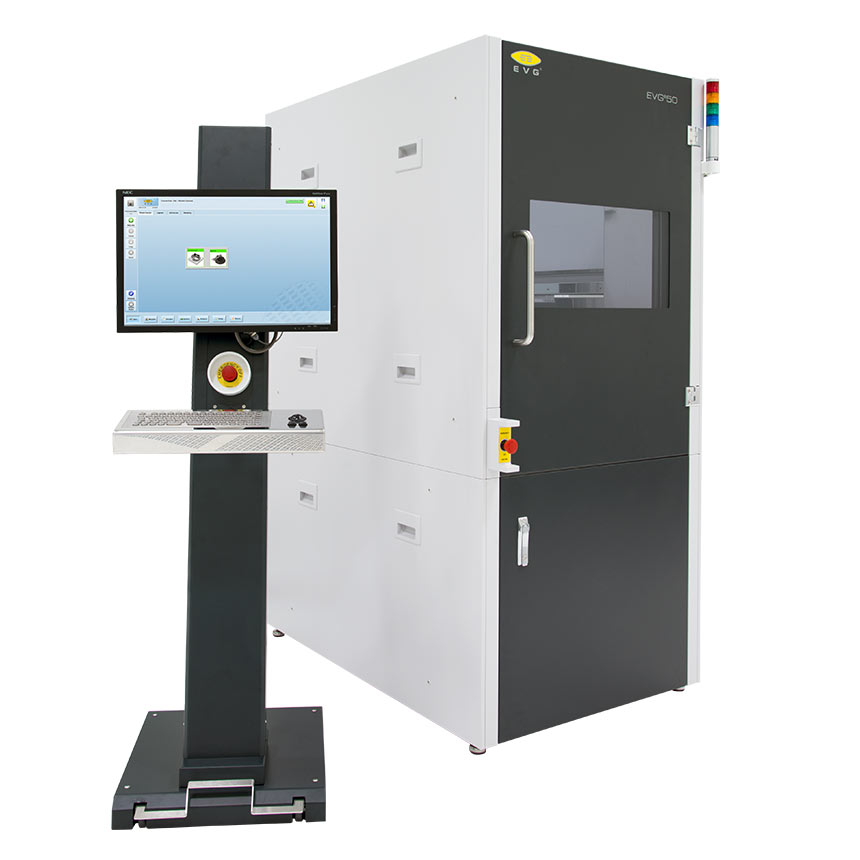
说明
Automated Metrology System
High-throughput, high-resolution metrology for bonded stacks and single wafers
The EVG50 (fully automated stand-alone tool) and the Inline Metrology Module (integrated in EVG's high-volume-manufacturing systems) offer highly accurate measurements at high speed, utilizing different measurement methods for a large number of applications. The tool's application range covers multi-layer thickness measurements for determination of the total thickness variation (TTV) of an intermediate layer, the inspection of bond interfaces as well as resist thickness measurement, and meets the most demanding requirements of the yield-driven semiconductor industry.
Features
Multi-layer metrology with industry-leading throughput and resolution
Multi-layer-thickness mapping
Bond interface inspection
Low contact edge handling
Particle free
Full-area accessible front- and backside
Self-calibrating for better system reproducibility and more productive time
Various output formats
100% production inspection
Explore our Technologies
光刻
纳米压印
键合
量测 EVG®20 EVG®40 NT EVG®40 NT2 EVG®40 D2W EVG®50
FAQ
提交需求
请填写必填信息,我们将在工作日尽快回复。